For years, the PV industry is being dominated by crystalline Si solar cells, with a market share of about 85 % of the total world solar cell production in 2008. Crystalline Si is still the only material that enables solar cell installations that function more than 20 years. Yet, if we want PV energy generation to be a relevant part of the total electrical energy generation, the cost of such a PV system must be reduced. Cutting down the costs is to be done by economies of scale (larger plants). But it also requires technological breakthroughs to reduce the cost of materials to manufacture cells and modules and the energy input to realize these components and to increase the energy conversion efficiency.
Mieke Van Bavel, Ivan Gordon, Valérie Depauw, imec, Leuven, Belgium
When analyzing the costs of present Si PV modules, it turns out that almost half of the price is currently due to the expensive electronic-grade Si in the solar cell. Hence, the main road that is being followed today is to reduce the thickness of the Si wafers that are used to produce the solar cells. Whereas in 2004, the standard wafer thickness in industry was still near 300 µm, it was 200 µm in 2008, and 180 µm is now becoming generally used. The Si content can be even further reduced to levels far below 1g/Wp by going to thin-film crystalline Si approaches where a thin film of Si (less than 20 µm) is deposited on a low-cost substrate. Promising results have been obtained with epitaxial solar cell concepts, where a low-cost highly doped crystalline Si substrate is being used on top of which an epitaxial Si layer is deposited. With such a technique, thin-film solar cells that compete with Si-wafer based cells can be provided. In a first approach, the technology is based on the creation of a thin crystalline-Si seed layer followed by epitaxial thickening of this seed layer. A second approach allows the development of epitaxy-free thin-film solar cells that allow an even larger price reduction.
Innovative seed layer approach
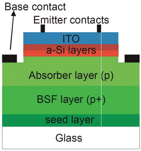
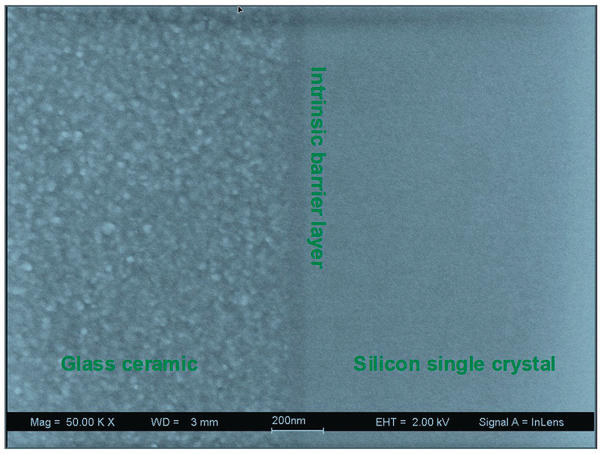
One way to create a crystalline-Si thin film on a non-Si substrate for solar cell applications is by using a seed layer approach: a thin crystalline-Si seed layer is first created, followed by epitaxial thickening of the layer. This is preferred over direct deposition of Si on the non-Si substrate, since this would result in amorphous or small-grained material. With the seed layer approach, promising thin-film polycrystalline solar cells with relatively large grain sizes have already been fabricated. Such cells could be of interest, since they combine the low-cost potential of a thin-film technology (like amorphous Si) with the material quality potential of a crystalline material. Imec made polycrystalline seed layers by using aluminum-induced crystallization (AIC) of amorphous Si and thermal chemical vapor deposition (CVD, at temperatures above 1000 °C) for the epitaxial thickening. Both alumina and glass-ceramic materials were used as a substrate. However, the problem with these polycrystalline layers is the high density of electrically active intragrain defects. These defects today limit the performance of the cells to 8 %. Improving these cells requires better AIC seed layer quality. The use of monocrystalline-Si seed layers could be beneficial, since it would enable simpler device processes, a higher process yield and a single-crystal-like efficiency because of an intrinsic higher material quality. To explore this idea, we have made 10 µm-thick monocrystalline-Si layers on transparent glass-ceramic substrates [1]. This was done by using monocrystalline-silicon seed layers on glass-ceramic substrates made by Corning. These seed layers are made by transferring 300 nm thin (001)-oriented Si single-crystal layers to a glass-ceramic substrate using Corning’s proprietary process that is based on anodic bonding and implant-induced separation [2]. A barrier layer, formed between the glass-ceramic substrate and the Si layer, prevents the Si layer from being contaminated by the glass-ceramic components. Subsequently, epitaxial thickening of the seed layers was realized in an atmospheric-pressure chemical vapor deposition (APCVD) system. From a crystallographic point of view, the monocrystalline layers have a much better quality than their polycrystalline counterparts obtained with the AIC approach in the same APCVD systems. These layers typically show an intragrain defect density of around 108 to 109 cm-2. The monocrystalline layers have overall defect densities as low as 105cm-2.
From these epitaxial layers, simple solar cell structures were made which did not integrate any light trapping features. Si solar cells on glass-ceramic reached efficiencies up to 7.5 %. For the short circuit current Jsc, which is due to the generation and collection of the light-generated carriers, a value of 23.4 mA/cm2 is reported. The open-circuit voltage Voc, which reflects the amount of recombination in the device, is 514 mV. However, efficiencies above 9 % should be realizable by using a more advanced contacting structure. In addition, we believe that the efficiency potential of these single-crystal Si thin films on glass-ceramics can compete with wafer-based Si solar cells. But this will require an optimized minority carrier diffusion length and an integrated efficient light-trapping scheme.
Epitaxy-free layer-transfer approach
The use of thin, high-quality layers of Si as the active solar cell material on low-cost carriers is an effective way to decrease the cost of photovoltaic electricity. High cell efficiencies have been demonstrated by layer-transfer processes, where thin layers of epitaxial Si are transferred to cheaper substrates [3]. Unfortunately, epitaxy is a very expensive processing step that seriously limits the intended cost reduction. Finding a way to by-pass epitaxy and still make high-quality thin films of Si would represent a real breakthrough. At the company, they have developed an innovative, cost-effective process that meets this expectation: we produced monocrystalline µm-thick films by annealing of macroporous Si and demonstrated the potential of this concept for large-area PV applications [4,5]. In fact, the technique is taken from the field of Si-on-nothing structures: it was found that upon annealing of specific arrays of macroporous Si at high temperatures, the macropores reorganise into one single void and leave a thin overlayer on top. The overlayer was reported to be monocrystalline and defect-free, suitable for Mosfet applications [6]. Its employment in PV applications is however not obvious: firstly, much larger areas (cm scale) have to be produced, and, secondly, the film has to be detached and bonded to a foreign substrate.
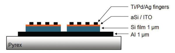
By using a 4-step approach, we successfully tuned this process to PV applications. In a first step, a very regular array of pores is etched in the Si wafer. To prepare the macroporous structure, we use deep-UV lithography and plasma etching, allowing a perfect control of pore ordering and size. In a second step, the wafers are annealed at 1150 °C in an argon or a hydrogen atmosphere, resulting in a 1 µm-thick film, as large as 5×5 cm2. In a third step, the film, still attached to its parent wafer, is bonded to a thick substrate for handling. We have used anodic bonding to glass, because this bond is direct, permanent and resistant to different chemicals and vacuum as well as heating. Besides, it is compatible with other materials that may be needed for a solar-cell process. After bonding, the thin film attached to glass can be easily pulled apart from its parent Si wafer and is ready for solar-cell processing. The parent wafer can be reused to provide new films. In a fourth and final step, a specific solar cell process is applied using temperatures not higher than 250 °C. The 1×1 cm2 solar cells have an amorphous Si/crystalline Si heterojunction emitter, with a full aluminum rear contact.
With this recipe, we made a first proof-of-concept solar cell with an energy conversion efficiency of 2.6 %. This result demonstrates the feasibility of the technique for making solar cells without resorting to epitaxy. The experiments also revealed some necessary precautions for material preparation, handling and solar-cell processing. E.g., as long as the film is attached to its parent Si wafer, the film requires to be protected from any electrostatic force, abrupt gas flows and vacuum pumping, in order to avoid early and undesired lift-off. Another necessary precaution is a perfect surface clean before annealing in order to minimize surface and structural defects during argon anneal. At this stage, the cell performance is rather low but leaves room for optimization. The low open circuit voltage Voc of 341 mV can be explained by the absence of rear-surface passivation and the high material resistivity. In addition, the short-circuit current Jsc, being 14 mA/cm2, is limited by the very thin absorber layer and by the absence in the cell design of schemes to absorb and trap more light in the material. And finally, the low fill factor of the cell is most likely limited by the presence of holes in the film, formed during transfer. Hence, optimization of the cell implies an increased film thickness, improved bonding (to avoid formation of holes), passivation of the rear-side and the addition of light-trapping schemes and surface texturing. Also, deep-UV lithography, used to prepare the macroporous structure, is a rather expensive technique and should eventually be replaced by a low-cost pore-patterning technique, like nanoimprint lithography. With these improvements, we believe that the epifree cells can reach comparable conversion efficiencies as their epi-based counterparts, without the cost-related bottleneck that epitaxy represents.
Conclusion
In an effort to bring down the Si content in solar cells, we have presented two novel thin-film crystalline Si solar cell concepts that make use of cheap non-Si substrates. A first approach is based on the creation of a thin crystalline-Si seed layer followed by epitaxial thickening of this seed layer. This has resulted in µm-thick monocrystalline-Si solar cells on glass-ceramic substrates with efficiencies up to 7.5 %. By implementing a more advanced contacting structure, by optimizing the minority carrier diffusion length and by integrating an efficient light trapping scheme, efficiencies comparable to wafer-based Si solar cells should become feasible. Although this is a very promising technique for making good-quality thin-film Si solar cells, the expensive epitaxial step could limit its cost-reduction potential. In a second approach, we propose to by-pass epitaxy by directly transferring a thin absorber layer of high-quality monocrystalline Si to a foreign low-cost substrate. The transfer is enabled by the reorganization of macroporous Si at high temperatures. Proof-of-concept solar cells have shown the feasibility of the technique to make good-quality solar cells without falling back on epitaxy. Conversion efficiencies are so far limited to 2.6 %, but improvements such as achieving a good passivation of the rear-side and incorporating specific light-trapping schemes will allow a significant increase of the cells performance.
References
[1] I. Gordon, S. Vallon, A. Mayolet, G. Beaucarne, and J. Poortmans, ‘Thin-film monocrystalline-silicon solar cells on transparent high-temperature glass-ceramic substrates’, Solar Energy Materials and Solar Cells 94 (2010) 381–385.
[2] R.G. Manley, G.L. Fenger, P.M. Meller, K.D. Hirschman, C.A. Kosik Williams,D.F. Dawson-Elli, J.G. Couillard, J.S. Cites, ‘Development of integrated electronics on silicon-on-glass (SiOG) substrate’, ECS Transactions 16 (9) (2008) 371–380.
[3] M. Reuter et al., ‘50 µm thin solar cells with 17.0% efficiency’, Sol. Energy Mater. Sol. Cells 93 (2009) 704–706.
[4] V. Depauw, I. Gordon, G. Beaucarne, J. Poortmans, R. Mertens and J.-P. Celis, ‘Proof of concept of an epitaxy-free layer-transfer process for silicon solar cells based on the reorganisation of macropores upon annealing’, Materials Science and Engineering, B 159–160 (2009) 286–290.
[5] V. Depauw, I. Gordon, G. Beaucarne, J. Poortmans, R. Mertens and J.-P. Celis, ‘Innovative lift-off solar cell made of monocrystalline-silicon thin film by annealing of ordered macropores’, Phys. Status Solidi C 6, No. 7 (2009) 1750–1753.
[6] T. Sato, et al., ‘Fabrication of Silicon-on-nothing structure by sustrate engineering using the empty-space-in-silicon formation technique’, Jpn. J. Appl. Phys. 43 (2004) 12–18.
Zusammenfassung
Die dringendste Forderung an die Technologie für Si-Solarzellen ist, sie billiger zu machen. Einer der Wege dorthin heißt: weniger Silizium. Bislang geschieht das durch immer dünnere Si-Wafer für die Module. Längerfristig lässt sich der Si-Verbrauch weiter reduzieren, indem man kristalline Si-Dünnfilme als aktives Zellenmaterial verwendet, mit Low-cost-Substraten als Carrier.
Dans la technologie des cellules solaires en silicium, l’urgence est de les rendre moins chères. L’une des voies est : moins de silicium. Jusque-là, on répond à cette exigence en fabriquant des semi-conducteurs au silicium de plus en plus fins pour les modules. A long terme, on peut encore réduire la consommation de silicium en utilisant des films minces au silicium en tant que matériau cellulaire actif avec des substrats low-cost agissant comme vecteur.
Ãëàâíîå òðåáîâàíèå, ïðåäúÿâëÿåìîå ê òåõíîëîãèÿì ïðîèçâîäñòâà êðåìíèåâûõ ñîëíå÷íûõ ýëåìåíòîâ, – ñäåëàòü èõ äåøåâëå. Îäíèì èç ïóòåé äîñòèæåíèÿ ýòîé öåëè ÿâëÿåòñÿ èñïîëüçîâàíèå ìåíüøåãî êîëè÷åñòâà êðåìíèÿ.  íàñòîÿùåå âðåìÿ ýòîãî äîáèâàþòñÿ çà ñ÷åò âñå áîëüøåãî óòîí÷åíèÿ êðåìíèåâûõ ïëàñòèí äëÿ ñîëíå÷íûõ ìîäóëåé. Åùå áîëüøå ñíèçèòü ïîòðåáëåíèå êðåìíèÿ íà äëèòåëüíûé ñðîê ìîæíî çà ñ÷åò èñïîëüçîâàíèÿ òîíêèõ êðèñòàëëè÷åñêèõ êðåìíèåâûõ ïëåíîê â êà÷åñòâå àêòèâíûõ ñîëíå÷íûõ ýëåìåíòîâ è íåäîðîãèõ ìàòåðèàëîâ â êà÷åñòâå ïîäëîæåê.
Share:


