Taken independently, the recent ratification pending adoption of another IEEE standard will each have significant effects on characterizing, debugging and testing multiple-die 3D chips. But taken together, the two standards will profoundly accelerate the quest for higher 3D chip yields, lower test development costs over the entire product lifecycle and quicken the time-to-market for system manufacturers.
Al Crouch, Asset InterTech, Richardson (USA)
The two standards are the IEEE 1149.7 Standard for Reduced-Pin and Enhanced-Functionality Test Access Port and Boundary-Scan Architecture and the IEEE P1687 Internal JTAG (IJTAG) standard for accessing on-chip embedded instrumentation. IEEE 1149.7 was ratified earlier in the year and IEEE P1687 is expected to be ratified during this year. Asset InterTech and its ScanWorks platform for embedded instrumentation are well positioned to take advantage of these standards to their fullest. ScanWorks is an open platform that can quickly accommodate new capabilities and Asset experts are in leadership positions on the working groups that have been developing both standards. Al Crouch, chief technologist core instrumentation of the company, is co-chairman of the P1687 working group and Adam Ley, chief technologist boundary scan, has served as the primary author and source of the test content in the 1149.7 standard.
Extending Moore’s law
Certain experts in the industry have asserted that 3D chip packages with multiple silicon die will be the most effective way for the industry to continue extending Moore’s law, which predicts a doubling of circuit density every 18 months to two years. The physics of chip fabrication process geometries below 90 nanometers (nm) are daunting. Some system manufacturers are finding it easier to stay with multiple die fabricated at a larger process geometry and placed in a 3D package than to move to chips processed at smaller submicron geometries. This has accentuated the critical nature of standards for characterizing, debugging and testing 3D chips before they are placed on circuit boards as well as validating, debugging and testing circuit boards after 3D chips have been placed on them. The two emerging standards – 1149.7 and P1687 – address this situation at the bare die, packaged chip and board levels.
For several years now, chip manufacturers have embedded test and measurement instrumentation into their devices in order to verify and test these devices from the inside out, instead of from the outside in. For instance, memory and logic built-in self test (BIST) engines, and internal scan have been embedded in chips for some time. A proprietary example of embedded instrumentation is Intel’s Interconnect Built-In Self Test (IBIST) which that company has been embedding into its next-generation chips and chipsets. The impetus behind this trend has been the increasing inadequacies of external probe-based test equipment, such as oscilloscopes, logic analyzers, in-circuit test (ICT), manufacturing defect analyzers (MDA), flying probe testers and others that rely on making physical contact with pins on chips or test pads on circuit boards. The state-of-the-art in the electronics industry today is such that this physical contact can disrupt and obfuscate characterization, validation and test measurements to the point where real faults or failures cannot be distinguished from those anomalies introduced by the physical contact. One solution is to eliminate physical contact from the test process by embedding instrumentation into chips and employing it in chip and board test applications.
As the need for embedded instrumentation has emerged, so too has the need for standard methods for accessing and automating these instruments, and for analyzing their output. As a result, representatives from companies across a wide swath of the electronics industry have come together to develop the 1149.7 and P1687 standards. At its most basic level, the IEEE 1149.7 standard maintains the access to chips and structures on circuit boards that the original boundary-scan standard (IEEE 1149.1) has provided since it was developed in the mid-1990s. (The boundary scan standard is also referred to as JTAG after the Joint Test Action Group which initiated development of the standard.) Boundary-scan access has been deployed in various applications, including circuit board test, the programming of chips in-system and others.
The 1149.7 working group has gone to great pains to ensure that this new standard is completely compatible with the original 1149.1 boundary-scan standard. As the name of the new standard implies, the intent of the working group was to develop a chip-level test access port (TAP) and associated architecture that would offer reduced pin-count from 1149.1 and enhanced functionality. Instead of the four-wire 1149.1 interface with an optional fifth wire, 1149.7’s TAP offers a two-signal solution, although an 1149.7 implementation may include all four (or five) signals.
In addition, the 1149.7 standard includes several architectural enhancements. For instance, support of multiple on-chip 1149.1 TAP controllers is possible under the 1149.7 standard. This and other features of the 1149.7 standard, such as its reduced pin count, a new glue-less star topology and compatibility with through-silicon vias (TSV), give engineers significantly enhanced capabilities for testing embedded cores or 3D chips individually and after they have been soldered onto a circuit board.
The P1687 IJTAG standard uses 1149.1 boundary scan for physical access to embedded instrumentation inside chips. Since embedded instrument IP (intellectual property) can come from a number of sources, such as chip suppliers, third-party providers, EDA tools or in-house design groups, P1687 is intended as a standard way of connecting, analyzing, describing and using embedded instrumentation no matter where the instrument has come from.
P1687 IJTAG enables a number of functions that will improve the testability of a single chip or multiple die in a 3D chip. For example, IJTAG could be used to automate and schedule the parallel operation of multiple embedded instruments. An embedded logic BIST engine for chip test might be operated simultaneously with a voltage monitor intended for yield analysis. The resulting simultaneous operation of these two embedded instruments could determine whether failures identified at the ATE- or board-levels correlated with voltage starvation.
Putting the two together
Deployed together in the same chip, 3D multiple-die device or circuit board, 1149.7 and P1687 form a potent solution for performing chip-level characterization, debug and test as well as board- and system-level validation, debug and test. In fact, the portability of this test methodology from the chip level all the way to the system level delivers huge benefits to manufacturers. Until now, during each phase of chip and system development, characterization, validation, debug and test routines were developed independently of each other. So, chip-level characterization and test routines would not migrate with the devices when they were deployed onto circuit boards and in systems. New test routines would be re-developed for circuit boards and again for systems. Embedded instrumentation and the interplay of 1149.7 and P1687 have the potential to change this so that test routines developed for instruments, cores and chips can migrate with those devices and be re-used throughout the entire lifecycle of systems. For example, P1687’s Procedural Description Language (PDL) functions much like the Boundary Scan Description Language (BSDL) of the 1149.1 standard. PDL allows instrument-level vectors to migrate and be re-used again and again. Better, more thorough tests would result as well as huge cost savings from significantly reduced test development efforts.
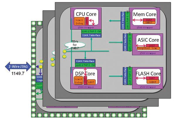
The block diagram shows how the 1149.7 and P1687 standards could be implemented in a 3D chip package, but the same principals would apply to single-die chips and board-level deployments. The multiple die stacked on top of one another in this illustration are connected vertically with through-silicon vias (represented by the yellow dot in the drawing) and a two-wire implementation of 1149.7. A broadcast star architecture on each die would connect each of the several cores on that die. A P1687 IJTAG interface on the embedded instruments would be used for standardized access and to coordinate all of their operations. By standardizing much of this scenario, third-party tools like the companies ScanWorks platform for embedded instrumentation can be deployed as a test executive to apply all sorts of test routines for chips, circuit boards and systems. And, since ScanWorks is an open platform, tools or processes from other third-parties can plug into the platform to extend its capabilities. Certainly new standards require time to be deployed and promulgate throughout the industry, but history has shown that open standards can provide the basis for markets to develop where technology suppliers innovate and compete with one another to provide the most cost-effective solutions possible. Certainly this is what will transpire in the marketplace for embedded instrumentation tools for single-die chips, complex SoCs, multiple-die 3D chips, circuit boards and systems.

Al Crouch is Chief Technology Officer – Core Instruments at Asset InterTech of Richardson, Texas and a Senior Mem-ber of the IEEE. He was formerly chief scientist and director of research and development at Ino-vys Corp. of Pleasanton, California, and Verigy Ltd. Of Cupertino, California. He has served as the vice chairman of the IEEE P1687 IJTAG working group that is developing the IJTAG standard and has contributed significantly to the hardware architecture definition. Over the last 20 years, he has accumulated vast experience in chip design-for-test at both Freescale Semiconductor (formerly Motorola) and Texas Instruments. Mr. Crouch has filed for more than 30 patents and been granted 15.
ZUSAMMENFASSUNG
Zwei neue IEEE-Standards stehen kurz vor ihrer Bestätigung, die jeweils für sich genommen schon erhebliche Auswirkungen auf die Charakterisierung, das Debugging und das Testen von 3D-Multi-Die-Chips haben werden. Kombiniert bieten sie Potenzial, die Ausbeute in der Herstellung zu erhöhen, die Testentwicklungskosten zu reduzieren und die Produkteinführungszeit für die Systemhersteller zu verkürzen.
Deux standards IEEE dont chacun aura un effet crucial sur la caractérisation, le débogage et le test de modules multipuces 3D sont sur le point d’être validés. Combinés, ils offrent le potentiel d’améliorer le rendement dans la production de puces 3D, de réduire les coûts de développement de test et de raccourcir les délais de mise sur le marché pour les fabricants systèmes.
Share:


