An inspection system now allows wafer edges to be monitored during the entire manufacturing process – both increasing yield and lowering costs, as the system prevents the processing of defective material. Moreover, because the sensor can be optionally integrated in existing process tools, it can be used in every production step.
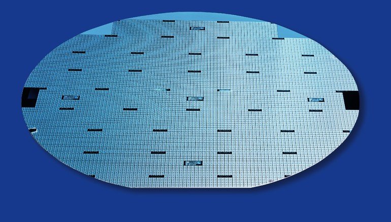
Today, the quality of wafers is often only checked at the start of production. However, the many processing steps put the material under a great deal of stress, particularly at the edge, and often cause quality issues. The high-speed surface inspection of the front, back and wafer edge is an efficient solution to this problem. This is necessary as chips are becoming ever thinner for use in modern IT and consumer electronics products, thus making them more vulnerable. Devices such as smartphones are gaining ever more functions, yet the amount of space for the hardware is limited. To meet the simultaneously increasing quality requirements, continuous inspection is required as early as the wafer manufacturing process.
Customized deployment for critical process steps
The EdgeScan from Isra Vision can be used as an OEM product throughout the entire process and for every type of wafer. It is compatible with all common process tools and is also available as a retrofit solution for existing machines. Moreover, the solution’s connection and results output comply with the SEMI standard. The sensor unit can be deployed in an individual manner depending on where in the process the components are under the most stress. During preadjustment, a line scan camera checks the edge of the wafer simultaneously from three sides. Its multiview technology, in which a prism deflects the image by 45 degrees, creates three views, making it possible to view the component from 360 degrees even at cycle times of just a few seconds.
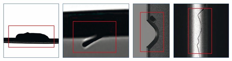
This kind of inspection is a result of the new awareness that problems often begin at the edge. Defects here can cause cracks and breaks. EdgeScan now allows the edge to be monitored throughout the entire production process. This solution complements conventional AOI systems that use a matrix camera, which have a limited field of vision and only inspect the surface, thereby enabling a complete inspection.
This high quality can be guaranteed throughout the entire manufacturing process due to the company’s solutions. For instance, CrackScan identifies micro cracks at the earliest possible stage and lays the groundwork for high-quality wafers and later chips. SurfQScan detects even the finest scratches on the polished, reflective surface of the finished wafer. And DicingScan enables inspection immediately following dicing, thereby covering a further process step that was previously not sufficiently monitored. Their portfolio of products for inspecting semiconductors enables the maximum customer satisfaction through the very highest quality.


